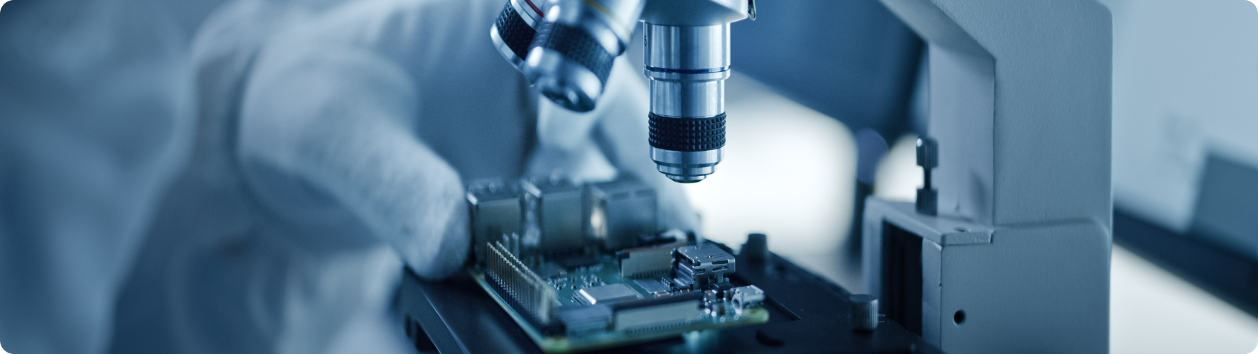
Material Experts
About Us
Our research center focuses on developing core technologies that lead various business areas pursued by
the company, primarily centered around semiconductor process component development.
The key goal of the center is to secure new technologies through advanced development and enhance existing businesses.
In the field of material development, we are conducting research on high-performance new materials used in semiconductor
processes, aiming to improve process efficiency and quality. Through the development of deposition technologies, we are
maximizing precision and durability in critical semiconductor manufacturing processes.
Building on our experience in manufacturing display process equipment, we are gradually automating component manufacturing
processes, achieving improved productivity and precision control in production processes.
The center focuses on the following four key areas of research.
Through research and development in these areas,
we are securing new technologies and commercializing them to
strengthen our competitiveness in the global market.
Our company continually invests heavily in R&D relative to revenue and has secured
specialized research personnel to enhance the operation of the research center. We pursue
relentless technological innovation through substantial R&D investment.
R&D investment as a percentage of revenue
(Unit: 1,000 KRW)
The research center is comprised of specialized personnel, including
Material Experts
AOI Technology
Engineers
Process Engineers
Automation System
Developers
Research personnel as a percentage of the total workforce
Our research center is dedicated to advanced technology research and development and holds key patents and intellectual property in various fields. We have achieved significant advancements in semiconductor process deposition technology, process automation solutions, and AOI (Automated Optical Inspection) technology, continuously strengthening our technological competitiveness in the market. These research achievements play a crucial role in securing technological superiority in both domestic and international markets, and we will continue contributing to industrial progress through innovative technology development.
Status of Intellectual Property Registrations
Edge Polishing System and Method
Edge Ring Outer Diameter Processing Device and Method
Edge Ring Processing System and Method
Edge Ring Inner Diameter Processing Device and Method
Tilting-Type Substrate Edge Polishing Device and Method
Disturbance-Reduction Roll-to-Roll Inspection System
Level-Adjustable Roll-to-Roll Inspection System
Manufacturing Method for a Component Containing a Silicon Carbide Layer
Substrate Polishing Device
Substrate Polishing Device with Contaminant Dispersion Prevention
Manufacturing Method for Large SiC Plate
Manufacturing Method for SiC Plate
Semiconductor Package Slimming Device and Method
Substrate Corner Processing Device
Substrate Processing Device
Panel Processing Device for Flat Panel Displays
Substrate Polishing Device and Method
Substrate Processing Device
Substrate Corner Processing Device
Semiconductor Package Slimming Device and Method
Edge Inspection Device and Method for Flat Panel Display Panels
Panel Polishing Device and Method
Substrate Polishing Device and Substrate Corner Polishing Method
Cell Scrap Removal Device and Method for Removing Cell Scrap
Panel Edge Inspection Device and Method
Polishing Device for Curved Glass Substrates
Polishing Wheel Flatness Correction Device, Panel Polishing Device, and Polishing Wheel Flatness Correction Method
Panel Manufacturing Device and Method
Clutch Device and Panel Transfer Device
Susceptor Manufacturing Device Equipped with a Cooling Fan
Susceptor Manufacturing Device Equipped with Means for Mixing and Heating Reaction Gases
Cell Scrap Removal Device
Rotating Device for Panel Polishing and Panel Rotation Method
Method for Manufacturing Cover Glass and Cover Glass Cutting Device
Cell Mounting Unit for Cell Scrap Removal Device
Cell Scrap Removal Device
Polishing Method for Flat Panel Display Panels
Device for Manufacturing a Susceptor through Mass-Transfer Controlled Reaction
Method and Device for Manufacturing a Susceptor through Mass-Transfer Controlled Reaction, and Susceptor Manufactured Thereby
Substrate Polishing Device and Method
Method for Manufacturing a Susceptor with a Concave Surface and Susceptor Manufactured Therefrom
Polishing Method for Flat Panel Display Panels
Substrate Polishing Device and Method
Wafer Chip Polishing Method
Substrate Polishing Device with Wheel Abrasion Compensation Capability
Substrate Picking Device and Method
Substrate Transfer Device
Polishing Method for Flat Panel Display Panels
Adjustable Table Device
Substrate Polishing Device and Method
Inspection Device and Method for Substrate Edges
Substrate Polishing Device and Method
Inspection Method and Device for Flat Panel Display Panels
Polishing Method for Flat Panel Display Panels
Scratch Inspection Device and Method
Substrate Polishing Device and Method
Edge Inspection Device and Method for Flat Panel Display Panels
Manufacturing Device for Flat Panel Display Panels
Inspection Device and Method for Flat Panel Display Panels
Integrated Inspection Device for Polishing Flat Panel Display Panels and Method
Manufacturing Device for Flat Panel Display Panels
Polishing Table and Method for Supporting Flat Panel Display Panels
Automatic Focusing Device and Method for Planar Compensation
Sawing Device for Semiconductor Package Manufacturing and Method for Manufacturing Semiconductor Packages
Manufacturing Device for Flat Panel Display Panels
Substrate Holder with a Venturi Tube and Sawing/Sorting Device
Sorting Table for Semiconductor Packages
Polishing and Inspection Device for Flat Panel Display Panels
Polishing and Inspection System for Flat Panel Display Panels
Manufacturing Device for Flat Panel Display Panels
Polishing Apparatus and Method for Flat Panel Display Panels
Substrate Transfer Device
Manufacturing Apparatus for Flat Panel Display Panels
Unloading Table and Semiconductor Package Unloading Device
Inspection Apparatus for Flat Panel Display Panels
Support Stage for Flat Panel Display Panels and Polishing Method
Polishing Apparatus for Flat Panel Display Panels and Method for Adjusting the Abrasion Stone
Polishing Method for Flat Panel Display Panels
Polishing Apparatus for Flat Panel Display Panels
Integrated Inspection Device for a Flat Panel Display Polishing Apparatus and Polishing Method
Method for Correcting the Abrasion Amount of a Grinding Stone and a Flat Panel Display Polishing Apparatus Capable of Correcting the Abrasion Amount of the Grinding Stone
Through continuous innovation, our research center aims to lead semiconductor process technology and
strengthen our competitiveness in the global market.
We are committed to pursuing advanced technology development, providing more advanced solutions to our
customers and partners.
We will lead future technologies and achieve results that exceed customer expectations.